 www.LED
  PLEASE NOTE!!!:
 Our German sites are much more detailed then our English sites. So please switch in our Germen sites and use the language translater (top right) with 60 languages.
4 designs of LEDs
The semiconductor crystal:
Silicium belongs to the most frequent elements of the earth's crust. It occurs however not purely, but as SiO2 (silicium dioxide or quartz)and must be converted by precipitation processes into pure silicium.Lattice defects in this crystal disturb however the movement of the electrons and in such a way that the crystalline pure silicium must be “cleaned” by a fusion procedure (Zohnenschmelz or Czochralski process) and "pulled" into large single crystals. These crystals has a diameter of 10-20 cm and a length of up to 2 meters. So a purity can be achieved by one foreign atom on 10 to high 9 Siliciumatomen.
This pure crystal is cut now into thin disks, called Wafern. Wafer costs today approx. around 1000, - Eur. The DOPING crucial for LEDs (addition of additives) can be achieved either with pulling the crystal or with the Wafern by vaporizing with 1000°C with the foreign atoms or by the bombardment with ions of the additive in small accelerators.
Now the endowed Wafern are cut into some hundred small “chips”, which exhibit a thickness of only approx. 250 µm. These tiny small and hardly with free eye visible pieces of semiconductor crystal are responsible for the light generation of our LED.
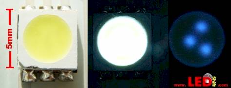 Many believe that the yellow shining layer, which is well recognized on the LED, is the semiconductor crystals. With the right admission of these SMD LED we used 2 polarisation filters. One can recognize clearly the 3 semiconductors chips.
|
Mainly however plastics and synthetic resin applications for the lens are used. In addition, glass or metal housings is used with bright LEDs. LEDs zum Einsatz.
The plastic body, which is formed like a lens and lies over the crystal, lowers the limit angle of the total reflexion and bundles, therefore increases the radiating power.
With stronger LEDs also glass lenses are used. Metal housings, mostly from aluminum, take over mainly the task of the heat dissipation, thus cooling.
 Thank you fo using |
1) Wired LEDs
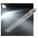
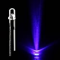
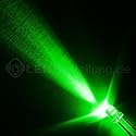
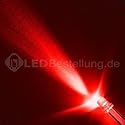
The Wired LED is at present still the most well-known LEDs because this design was already used for a very long time in electronics. They were mostly used however only as control small lamps.
When the luminous efficiency of semiconductor crystals became better and better, the wired LEDs became generally accepted in the lighting industry. Several wired LED in summary, are found nowadays in LED SPOTS, LED tubes, LED modules and LED chains.
The advantage of wired LEDs exists in very favorable production in the small heat emission and that they can very simply soldered. The most usual models of wired LEDs/strong> are 3mm, 5mm and 10mm diameter.
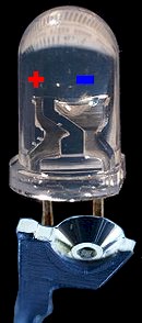
The reflector tub in that semiconductor crystal is embedded, is also the short leg of a wired LED and also the MINUS - (cathode). A further distinguishing feature for the Minusseite of a Bedrahteten LED is an easy flattening of the plastic shroud on this side.
Wired LEDs are produced in all colors also in RGB (RED, GREEN, BLUE). Either with automatic color change or automatic dialable. The automatic dialcash possess 4 legs (pin).
|
With these SMD LED one can recognize the 4 semiconductors Chip´s under the yellow shining layer
|
2) SMD LEDs ( Surface Mounted Device )
|
Löten von SMD LEDs
|
SMD LEDs possess not as the wired LED small wire connections, caled pins, but by means of solderable mating surfaces are soldered directly on the printed circuit board. Who does not use a printed circuit board, can naturally also wire connections on the mating surfaces solder.
Several SMD LED in summary, find nowadays with LED SPOTS, LED tubes and LED modules application.
SMD LED are made in different sizes, shapes of the housing and light-current strengths. By the enormous luminosity of some SMD LED, with which usually 3 or 4 semiconductor crystals are embedded in a SMD LED, they are used as flashlight LED in mobile phones or very compact digital cameras. Also in the automobile industry SMD LED are used for turn signals, stop light or daily headlight. SMD LEDs are produced in all colors also in RGB (RED, GREEN, BLUE).
 LED Stripes |
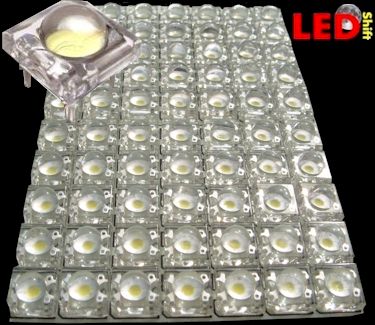
3) Superflux LEDs ( Spider LEDs )
One could see superflux LED (or Spider LED called) as advancement of the wired LED.
They possess a large reflected beam angle and send their light laminar and are therefore better suitable for surface lighting. The four contact contacts (pin) do not only make a better heat dissipation and thus a high life span possible, but they can be headed also separately. Spider LED contains up to 4 semiconductor crystals (chips).
These advantages make those for superflux LED a perfect multi-chip carrier with infinitely many ranges of application.
Superflux are used in LED bulbs, LED tubes, LED modules and ever more frequently in addition, in the autolighting industry.
Here we know them as Soffitten in many different sizes and colors. In the advertising industry they are used e.g. for signature lighting or dia. assemblies.
Superflux LEDs are used for turn signals, stop light or daily headlight. SMD LEDs are produced in all colors also in RGB (RED, GREEN, BLUE).
4) CBO LEDs ( Chip on Board )/ Power LEDs
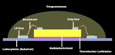 CBO LEDs the semiconductor crystals is directly contacted at the plate.
The chip on board technology is clearly the innovativste range of the semiconductor technology. With this technology the individual LED chips with the assistance of fully automatic Bondern are set directly on a gilded printed circuit board. This special procedure is called “Bonding”. Subsequently, contacting is made to the antipole by a gold or aluminum wire.
The COB technology makes chip densities possible of up to 70 Chips/cm2!!! and made possible as an enormous intensity with even annunciator and offers many ranges of application with boundless organization freedom infinitely in connection with differently substrates as e.g. flexible printed circuit boards and ceramics.
Durch Chip On Board Technik kann auch eine optimale Wärmeableitung erreicht werden, welches die Lebensdauer einer LED enorm beeinflusst.
By chip on board technology can be achieved also an optimal heat dissipation, which affects the life span an LED enormously. To the COB LEDs belongs nearly all power LED variants. Zu den COB LEDs gehören fast alle Power LED Varianten.
COB LEDs are produced in all colors also in RGB (RED, GREEN, BLUE).
Around the semiconductor designs to complete one should mention actually also still the fifth “design”, i.e. the OLEDs (click here for Oled info.) Um die Halbleiter-Bauformen zu vervollständigen sollte man eigentlich auch noch die fünfte "Bauform" erwähnen, nämlich die OLEDs(klick here for Oled info).

| AGB Ledshift | LED Function | LED Producer | LED Distributor | LED Events | LED Company Entry | LEDS | Sitemap | Contact | |
|
|
© Markus Kottas, Heldenberg Ltd.2018


